
High current regulator
7805
Pinout
| Pin | Function |
|---|---|
| IN | Regulator input. It receives the input voltage through Re, the resistor that sets when the pass transistor starts conducting. |
| GND | Common terminal and reference for the 5 V output. |
| OUT | Regulated 5 V output. It ties to the collector of Q1, which supplies the bulk of the load current. |
MC7805
The 7805 (here in its MC7805 version) is a three-terminal linear voltage regulator from the 78xx family. It delivers a fixed 5 V output, but its maximum current is limited to 1 A, and only with adequate heat sinking.
When the load asks for more than the regulator can give, there is no need to switch families: it is enough to boost it with a PNP pass transistor. In this circuit an MJ2955 (a 15 A, 115 W PNP, the complement of the classic 2N3055) takes care of the bulk of the current while the 7805 keeps doing what it does best: holding the output at 5 V. Together they deliver on the order of 5 A while keeping the regulation of the IC.
How the circuit works
The idea is simple: the regulator stays in charge, but stops carrying all the current.
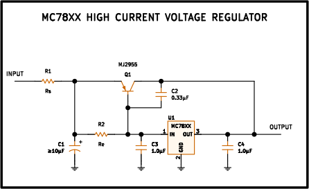
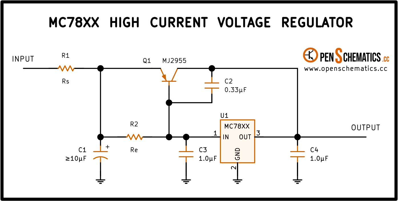
All of the circuit’s current comes in through Rs and reaches a common node with two paths hanging off it: the emitter of Q1 and resistor Re, which feeds the regulator’s IN pin. In other words, Re sits between the emitter and the base of Q1 (the base connects to the same node as IN), so the voltage drop across Re is exactly the transistor’s base-emitter voltage.
With light loads the regulator draws little current, the drop across Re does not reach the PNP’s (about 0.6-0.7 V) and Q1 stays off: the circuit behaves like a plain 7805. As the load grows, the current through Re rises, the drop climbs and, once it reaches , Q1 starts conducting and supplies through its collector the current the output is missing. From that point on the voltage across Re is pinned at : the regulator’s current stays “anchored” near that value and all the excess the load asks for comes from the transistor, not from the IC.
The regulator, meanwhile, keeps sensing the output and adjusting: if the voltage sags, it draws a bit more base current through Re, Q1 conducts harder and the output returns to 5 V. The 7805 goes from being the pass element to being the driver of a much bigger transistor.
The rest of the parts play supporting roles:
- C1 () is the reservoir on the unregulated input: it absorbs the current peaks, which can now reach several amps.
- C3 () decouples the regulator’s IN pin, as its datasheet asks for when the IC sits far from the input filter.
- C4 () improves the transient response at the output.
- C2 () bridges the output and the IN node, that is, the base-collector junction of Q1: it damps the loop formed by the regulator and the transistor and helps prevent oscillation.
One important warning: this circuit is not short circuit proof. The 7805’s internal protections (current limiting, thermal shutdown) only look after the IC itself; Q1 is outside that loop and, if the output is shorted, nothing limits the current it delivers.
Application design
1. Conduction threshold of Q1. This is the only thing Re sets. The current through it gets anchored at:
With and we get : the 7805 works on its own up to near its limit and Q1 takes over from there.
2. Current split. That Re current divides between what the regulator draws and the transistor’s base, and the collector multiplies the latter by the gain:
The MJ2955 has to at ; it is wise to design for the worst case, . For a output with :
That means the transistor provides and only flows through the 7805, within its 1 A limit. Lowering Re brings the transistor in earlier but unloads the IC further; raising it makes the 7805 take on more work.
3. Power in Re. Once Q1 conducts, Re permanently takes :
A rating of at least is advisable.
4. Q1 dissipation. This is the critical point of the circuit: the transistor swallows the input-output differential at full current.
With and that is about : a heatsink is mandatory. The MJ2955’s 115 W is its maximum with the case at 25 °C, a figure never reached in practice.
5. Minimum input voltage. The pass transistor adds its to the minimum differential the regulator already requires:
With a typical dropout of around 2 V that gives , plus whatever drops across Rs.
6. Rs. It sits in series with the input and carries the total current (the regulator’s plus the transistor’s), so its value must stay in the range of tens of milliohms: every means of drop and dissipated at 5 A. Its drop is proportional to the total current, which also makes it the natural place to add sensing if you want to give the circuit the short circuit protection it lacks.
Other applications
Beyond the current boost explained here, the 7805 shows up in many circuits: fixed 5 V supplies, local on-board regulation, current sources or adjustable regulators. Some of the most common:
- 5 V supply for logic and microcontrollers. Its classic use: delivering a stable 5 V to digital circuits from a larger unregulated source.
- Local on-board regulation. A regulator next to each board or block of the system, instead of a single central supply, to cut down noise and wiring drops.
- Constant current source. With a single resistor between OUT and GND, the regulator sets the current instead of the voltage.
- Adjustable output regulator. By lifting its common pin with a divider or a diode, the output rises above the nominal 5 V.
- Basic bench power supply. With a transformer and a bridge rectifier, it provides a ready-to-use 5 V output for the workbench.
References and further reading
- PDF7805 datasheet
This is the main source this article was created from.
- WEB
- WEB