
USB to UART converter
CH340G
Pinout
| Pin | Function |
|---|---|
| Pin 1 (GND) | Common ground, connected directly to the USB bus ground. |
| Pin 2 (TXD) | Asynchronous serial data output (TTL level). |
| Pin 3 (RXD) | Asynchronous serial data input, with built-in controllable pull-up and pull-down resistors. |
| Pin 4 (V3) | Internal 3.3 V regulator node. With VCC = 5 V it connects to a 0.1 µF decoupling capacitor; with VCC = 3.3 V it is shorted to VCC. |
| Pin 5 (UD+) | USB D+ data line. Connects directly to the connector without a series resistor. |
| Pin 6 (UD−) | USB D− data line. Connects directly to the connector without a series resistor. |
| Pin 7 (XI) | Crystal oscillator input. Requires an external 12 MHz crystal with load capacitors. |
| Pin 8 (XO) | Crystal oscillator output. Connects to the other end of the 12 MHz crystal with its load capacitor. |
| Pin 9 (CTS#) | MODEM contact input signal, "clear to send", active low. |
| Pin 10 (DSR#) | MODEM contact input signal, "data set ready", active low. |
| Pin 11 (RI#) | MODEM contact input signal, ring indicator, active low. |
| Pin 12 (DCD#) | MODEM contact input signal, carrier detect, active low. |
| Pin 13 (DTR#) | MODEM contact output signal, "data terminal ready", active low. |
| Pin 14 (RTS#) | MODEM contact output signal, "request to send", active low. |
| Pin 15 (R232) | Auxiliary RS232 function enable input, active high, with internal pull-down. Only sampled once after power-on reset. |
| Pin 16 (VCC) | Positive power supply input (5 V or 3.3 V). Requires an external 0.1 µF decoupling capacitor. |
USB to UART converter with CH340G
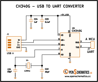
This circuit turns a USB port into an asynchronous TTL serial port (UART). Once plugged into the computer it shows up as a virtual COM port, and everything sent or received through it travels as logic-level serial data (0 V / VCC) on the TXD and RXD lines of connector J2. It is the classic way to program microcontrollers (ESP8266, ESP32, AVR, STM32…), open a debug console, or add a USB port to any legacy peripheral with a serial output.
The core of the circuit is the CH340G, a USB-to-serial adapter chip from WCH compliant with full-speed USB 2.0. The USB transceiver, the identification pull-up and the transmit/receive buffer are all integrated on-chip, so the external circuitry is reduced to the clock crystal, three decoupling capacitors and the two connectors.
Package SOP-16.
How it works
The CH340G integrates a full USB transceiver, a hardware full-duplex UART engine and all the control logic. When plugged into the computer it enumerates as a USB device, the operating system loads the VCP (Virtual COM Port) driver and creates a virtual serial port. From then on, characters the application writes to the COM port come out of the chip’s TXD pin at TTL level, and characters arriving on RXD are sent back to the computer over USB.
Power supply
The circuit is powered from the USB bus, which delivers 5 V on the VBUS pin of connector J1. This voltage feeds the VCC pin (pin 16) of the CH340G and is also brought out as the auxiliary +5V rail on the UART connector J2. Capacitor C24 (1 µF) filters the bus, and C23 (0.1 µF) decouples the VCC pin at high frequency.
The V3 pin (pin 4) is the internal regulator node that generates the 3.3 V rail for the USB transceiver. When the chip is powered from 5 V, this pin only needs a 0.1 µF decoupling capacitor to ground. If the chip is instead powered from 3.3 V, V3 is shorted to VCC and 3.3 V is fed into both.
12 MHz clock
The CH340G needs an external 12 MHz clock for the USB engine and the baud rate generator. Crystal X4 is connected between pins XI (pin 7) and XO (pin 8), with load capacitors C21 and C22 (33 pF) to ground on each end. This oscillator is the only reason the chip comes in SOP-16 rather than SOP-8: the CH340C, CH340N and other variants integrate the clock and do without these three components.
Crystal tolerance is critical for the transmitter baud rate error: the datasheet guarantees less than 0.3 % error on parts with an external crystal (CH340G/T/R), versus 1.8 % for those relying on the internal clock.
USB interface
Pins UD+ (pin 5) and UD− (pin 6) connect directly to the D+ and D− lines of USB connector J1, with no series resistors. The chip itself provides the 1.5 kΩ pull-up on D+ that identifies the device as full-speed to the host.
Serial interface
Connector J2 exposes the four typical signals of a USB-TTL adapter: GND, TXD, RXD and +5V. TXD and RXD run at TTL level (0 V / 5 V, or 0 V / 3.3 V if the chip is powered at 3.3 V), with standard framing: 1 start bit, 5–8 data bits, 1 or 2 stop bits and optional parity. Supported baud rates range from 50 bps to 2 Mbps.
The additional MODEM signals (CTS#, DSR#, RI#, DCD#, DTR#, RTS#) are left unconnected in this basic schematic. They can be left floating when unused; the PC software can read or drive them if a given board brings them out to another header — useful, for example, to control the reset and bootloader-entry sequence of development boards.
Choosing the crystal and its capacitors
The crystal must be exactly 12 MHz (the datasheet accepts 11.98–12.02 MHz). It is the only reference that sets the CH340G’s internal frequency, so a crystal out of tolerance translates directly into baud rate error and dropped communication with the host.
Load capacitor values (C21 and C22) depend on the type of crystal:
| Crystal type | Typical load | C21 / C22 |
|---|---|---|
| Standard quartz | 12–20 pF | 33 pF |
| Low-cost ceramic | 15–30 pF | 47 pF (per manufacturer) |
For quartz crystals, 33 pF is the value recommended by WCH and works with the vast majority of commercial parts. For a ceramic resonator, use the value specified by its manufacturer.
USB connector and protection
Connector J1 is a USB type A (male or female depending on the intended use). Its four pins are:
| Pin | Signal | Function |
|---|---|---|
| 1 | VBUS | +5 V from the host |
| 2 | D− | Negative data line |
| 3 | D+ | Positive data line |
| 4 | GND | Ground |
For a basic adapter like this one, the computer’s USB port already provides overcurrent protection (a resettable fuse), but in builds where the circuit is exposed to electrostatic discharge it is worth adding a TVS array (such as the USBLC6-2SC6) across D+, D− and VBUS.
Baud rates and accuracy
The CH340G generates all standard baud rates internally by dividing the 12 MHz clock. The usual values (9600, 19200, 38400, 57600, 115200, 230400, 460800…) are supported directly, along with non-standard rates such as 250000 (used by DMX) or up to 2 Mbps.
The overall link error is the sum of the crystal error and the internal divider error. With a ±20 ppm crystal, this stays well below the ±2 % margin tolerated by any UART, and communication is reliable even at 921600 bps.
Other applications
Beyond acting as a generic USB-TTL cable, this circuit is the basis of:
- Microcontroller programmers. Many ESP8266/ESP32 modules, Arduino Nano boards and Arduino UNO clones use the CH340G (or its CH340C variant without a crystal) as the built-in USB-serial bridge; DTR# and RTS# are used to drive the reset and bootloader-entry sequence.
- Legacy serial ports on modern PCs. Add a COM port to a computer with only USB, to talk to lab instruments, scales, barcode scanners or other legacy serial peripherals.
- Debug console. Read the
printfmessages of a microcontroller from a serial terminal on the computer during development. - USB to RS232 and RS485 adapters. By adding a level shifter (MAX232, MAX485), the CH340G becomes the front end of a USB-to-RS232 or USB-to-RS485 adapter, exactly as shown in the application circuits of the datasheet.
- KVM and serial automation. USB interface for devices that control other machines over a serial console (routers, switches, servers) from a computer or an embedded system.
References and further reading
- PDFCH340G datasheet
This is the main source this article was created from.
- WEB
- WEB